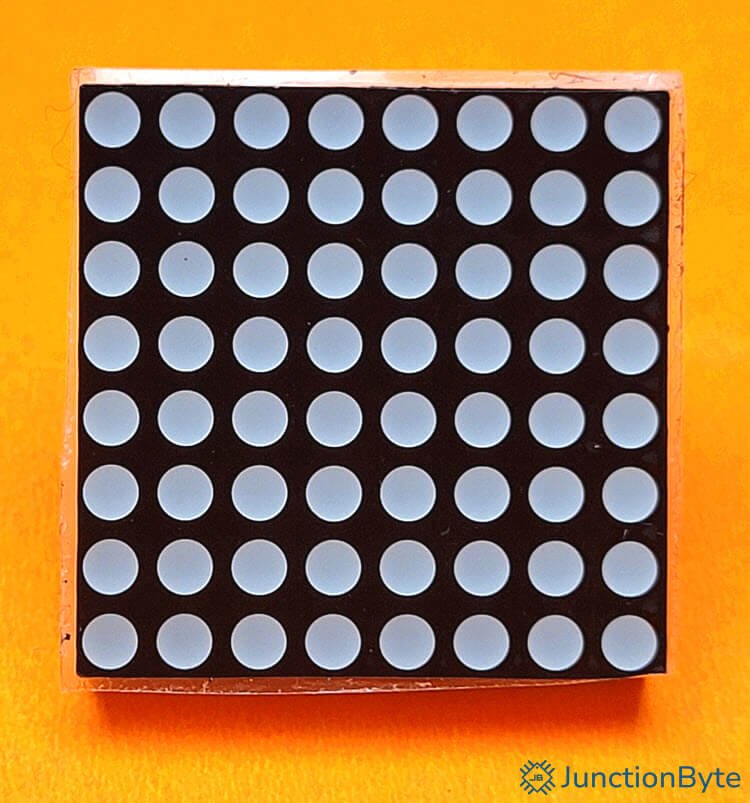
LED Dot Matrix Displays are still a popular way to show information, either on a small scale such as clocks, or on a large scale such as digital bill-boards. The 8×8 LED Dot Matrix is the simplest of the bunch with LEDs (usually red) arranged in a grid of 8 rows and 8 columns. Instead of directly driving the LED Matrix, we often use special ICs (known as driver ICs) to control the LEDs. One such popular LED Driver IC is the MAX7219. It simplifies LED control by handling multiplexing and brightness internally. In this guide, let us learn how to interface and control MAX7219 8×8 LED Matrix with STM32G4 microcontroller (both single and cascaded).
The MAX7219 handles data serially through the SPI protocol. So, we will see how to configure the SPI pins of the STM32G431CBU6 MCU in the STM32CubeIDE. We will also write a driver for the MAX7219 Module that is compatible with STM32G4 MCUs (you can easily modify this driver to work with any STM32 MCU).
Before starting, I would like to remind you that I already made a couple of “introductory” STM32G4 guides that cover some important basics. This includes setting up the STM32CubeIDE for pin configuration, clock tree, as well as generating the starting code with STM32 HAL framework.
I also explained how to program (or upload the binary to) an STM32G4 MCU using ST-Link as well as USB DFU. While I will cover some of the essentials necessary for this project here, I strongly advise you to check those guides for more in-depth information.
Here’s the links to those guides:
- Introduction to STM32G4
- Getting Started with STM32CubeIDE and STM32G4
- How to Program STM32G4 in PlatformIO?
Required Components and Tools
Hardware Components
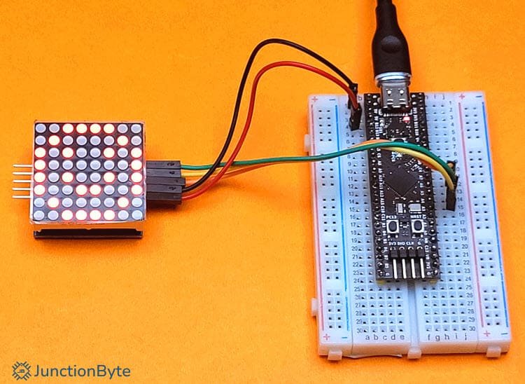
You need an STM32G4 development board to control the LED matrix modules in this project. In my case, I will be working with a low-cost WeAct Studios STM32G431 Core Board that has the STM32G431CBU6 MCU on-board.
With a single MAX7219 8×8 LED Dot Matrix module, you can build the basic version of the project. This module consists of an 8×8 matrix of LEDs mounted directly on a PCB along with a MAX7219 driver chip. You can use the single module with the STM32 board and test display output without any complexity.
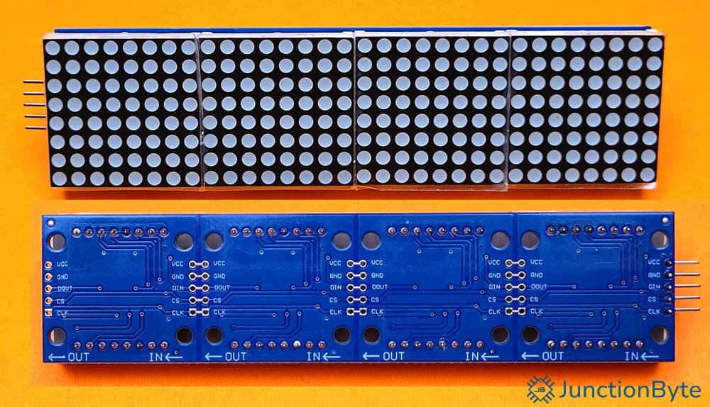
The benefit of MAX7219 Modules is that you can easily cascade them to create larger displays without increasing the wiring complexity between the STM32 and the display units.
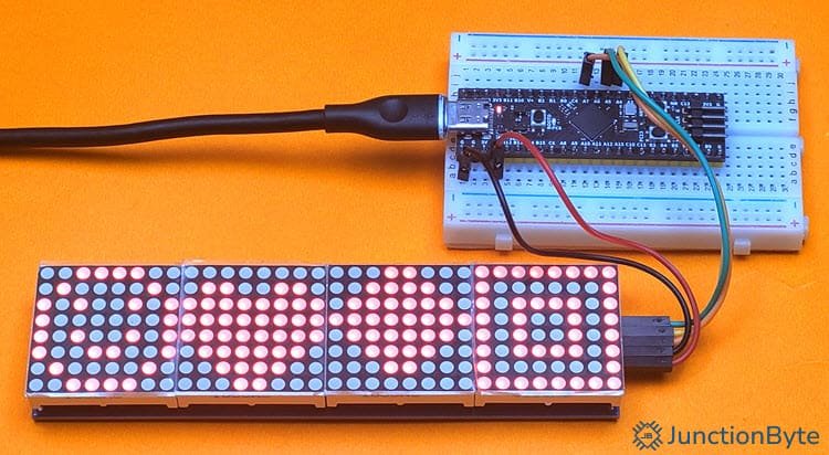
For an expanded display, you need the 4-Channel Cascaded MAX7219 Module, essentially 4 MAX7219 Modules connected back-to-back and uses the same 3 wires for data.
You can get debugger tools like ST-Link that allow you to program and debug the STM32G4 MCU in real-time. Here’s a list of all the hardware you need:
- STM32G4 Development Board
- MAX7219 88 LED Dot Matrix Display Module
- 4-Channel Cascaded MAX7219 8×8 LED Dot Matrix Display Module
- Breadboard
- Jumper Wires
- External 5V Power Supply (for cascaded module)
Software Tools
Coming to the software, I will be using the STM32CubeIDE as the main platform for developing, compiling, and debugging the firmware for this project. It combines device configuration (pins and clock), code editing, project management, and debugging into a single workspace.
STM32 HAL libraries provide an abstraction layer between the hardware and the application code. For uploading the code without ST-Link, you will need the STM32CubeProgrammer.
So, here’s a list of software you will need:
- STM32CubeIDE
- STM32 HAL Library (in my case, for STM32G4)
- ST-Link Drivers
- STM32CubeProgrammer
Communication Protocol Between STM32G4 and MAX7219
MAX7219 modules use SPI to receive display data from a microcontroller (in this case the STM32G431CBU6). In an SPI system, one device acts as the Controller of the bus (STM32G4 MCU) and others operate as Peripherals (MAX7219). The Controller is responsible for all the timing and data flow while the Peripherals respond to the instructions from the Controller.
SPI communication is a synchronous data transfer, which means a clock signal defines when data bits move between devices.
During normal operation, the STM32 MCU sends two bytes to the MAX7219 during each SPI transaction. The first byte specifies the register address within the MAX7219, and the second byte contains the corresponding data.
After sending both bytes, the MCU toggles the CS line HIGH momentarily to latch the data into the MAX7219 registers. Each transaction updates one internal register (decode mode, scan limit, intensity, or a particular row’s display data).
When cascading multiple MAX7219 modules, the first 16 bits will reach the last module in the cascade (farthest from the MCU). Each subsequent 16-bit segment moves one module closer to the STM32 until all modules receive their respective instructions.
Signal Lines Between MAX7219 and STM32G4
Three main signal lines create the connection between the STM32G4 MCU and the MAX7219 module. These are:
- DIN (Data In)
- CLK (Clock)
- LOAD/CS (Chip Select)
The DIN line carries the serial data bits from the STM32 to the MAX7219. This line remains stable except during active SPI data transmission. Bits shift into the MAX7219 on the rising edge of the CLK signal.
The CLK line provides the clock signal (a continuous stream of pulses) that synchronizes the transmission of data bits. Each pulse shifts one bit into the MAX7219’s internal shift register. We don’t have to worry about the clock as the SPI peripheral in the STM32 automatically generates these pulses based on the SPI clock speed configuration.
Finally, the LOAD or CS line signals the MAX7219 when to latch the received data into its active control registers. When the STM32 finishes sending 16 bits, it drives the CS line HIGH for a brief moment. This action triggers the MAX7219 to apply the newly received data to its internal logic and display outputs.
Hardware Setup to Control MAX7219 8×8 LED Matrix with STM32G4
If you look at the basic MAX7219 8×8 LED Matrix Module, it has five important pins: VCC, GND, DIN, CLK, and CS (LOAD). The following table shows the connections between the MAX7219 and the STM32G4 Development Board:
| MAX7219 | STM32G4 |
| VCC | 5V |
| GND | GND |
| DIN | PA7 |
| CLK | PA5 |
| CS | PA4 |
Connect the VCC and GND pins of the MAX7219 to the 5V output and ground pins of the STM32 board respectively. Although the VCC of the MAX7219 is 5V (it is necessary to drive all LEDs correctly), the MAX7219 accepts 3.3V signals on DIN, CLK, and CS.
Next, wire the DIN pin of the MAX7219 to the STM32 SPI MOSI line. On the STM32G431CBU6, the default SPI1 MOSI pin is PA7. Connect the CLK pin of the MAX7219 to the STM32’s SPI SCK line, which is PA5 for SPI1. Finally, connect the CS (LOAD) pin of the MAX7219 to a free GPIO pin, for example, PA4. We will use this pin for manual chip-select control from software.
Cascading MAX7219 Modules
If you have a proper, readymade 4-Channel MAX7219 88 LED Matrix, then the wiring is already done for you. Each module shares CLK and CS signals but passes its received data down the line through DOUT (Data Out). The DOUT of the first module connects to the DIN of the second module and so on.
STM32CubeIDE Project Setup
Create a New Project
Let us start the firmware development. Open STM32CubeIDE and select File -> New -> STM32 Project. The IDE will open the “STM32 Target Selector” window. Enter “STM32G431CBU6” in the search bar (Commercial Part Number) and select it from the results on the right.
After selecting the correct MCU, click “Next” to proceed. Give the project a unique name, such as “MAX7219-LED-Matrix” or something similar. Choose a suitable project location on your computer and you can leave the rest of the options at their default.
Once the project environment loads, the device configuration tool will open automatically where you can configure all MCU peripherals needed for the project.
Configure the Peripherals
External Clock
The IDE should open the “Pinout & Configuration” tab. Expand “System Core” and click on “RCC.” Set the High Speed Clock (HSE)” to “Crystal/Ceramic Resonator.”
Move to “SYS” and set the “Debug” to “Serial Wire.” This is important if you want to debug and program the MCU using ST-LINK.
SPI Peripheral
Now, expand the “Connectivity” section on the left panel and click on “SPI1” and set the mode to “Full-Duplex Master” because the STM32 will only transmit data to the MAX7219.
The IDE will automatically set default pin assignments for SPI1, which is SCK (Serial Clock) to PA5, MISO (Master In Slave Out) to PA6, and MOSI (Master Out Slave In) to PA7. However, you can manually reassign these pins. Just press Ctrl and click and hold the default pin to see the list of possible alternatives. I will leave them as they are.
Next, in the “Configuration” panel that appears below, set the data size to 8 bits, which matches the communication protocol of the MAX7219.
Now we have to adjust the “Prescaler” to keep the SPI clock under 10 MHz, which is the MAX7219’s maximum supported speed (the SPI clock speed can be between 2 MHz and 10 MHz). If we are running the STM32G431CBU6 at the maximum clock speed i.e., 170 MHz, we can select the prescaler of 16 to achieve ~10.6 MHz (170/16).
For clock polarity (CPOL), set it to “Low,” and for clock phase (CPHA), choose “1 Edge.” This will place the MAX7219 in SPI Mode 0.
Going back to the SPI Mode Configuration, leave the “Hardware NSS Signal” as “Disable.” This is because MAX7219 requires manual CS control and so, we will use a GPIO Pin as a CS Pin for manual software control. Also make sure that the “NSS Signal Type” under “Advanced Parameter” Settings” tab is set to “Software.”
Configure GPIO for CS
Locate a free GPIO pin in the pinout view. As PA4 is close to the rest of the SPI pins and is free on my development board, I will be using this as the CS Pins. So, click on “PA4” and assign it as “GPIO_Output.” Label it clearly (e.g., MAX7219_CS) for easy reference in code.
Clock Configuration
Although we enabled the crystal as the external clock, we still haven’t explicitly set it as default. So, click on the “Clock Configuration” and select HSE (external crystal) as the primary clock source (PLL Source Mux).
Since we want maximum MCU performance, we will make the System Clock (SYSCLK) to run at 170 MHz. For this, set the “HCLK” value as 170 (MHz) and hit enter. The IDE will automatically adjust different parameters and set the SYSCLK as 170 MHz.
Generate Project Code
After completing all configurations, save the Device Configuration options by pressing “Ctrl+s” and the IDE will ask whether to generate code or not. Click on “Yes.” The IDE will now ask whether to switch to C/C++ perspective and once again, click on “Yes.” Alternatively, you can select Project -> Generate Code to generate the code.
Next, we will develop the MAX7219 driver.
MAX7219 LED Matrix Driver Code Implementation
I already talked about this in the previous “How to Interface PCF8574 I2C LCD with STM32G4 MCU” guide.
In the “Project Explorer”, right-click the “Drivers” folder and add a folder (New -> Folder). Let us call this User_Driver. Right-click this new folder (User_Driver) and add two more folders and name them “Inc” and “Src.”
Now, right-click the “Inc” folder and add a new header file (New -> Header File) and give it the name “MAX7219_LED_Matrix.h” (don’t forget the .h extension).
Similarly, “PCF8574_I2C_LCD.c” file in the Src folder (this time, create a Source File i.e., New -> Source File). These files will contain all MAX7219-specific functions and definitions.
MAX7219 LED Matrix Driver Header Code
Open the “MAX7219_LED_Matrix.h” and delete any auto-generated data. Copy and paste the following code and save the file. I have added comments for all the sections for easy understanding.
/* MAX7219_LED_Matrix.h */
#ifndef INC_MAX7219_LED_MATRIX_H_
#define INC_MAX7219_LED_MATRIX_H_

#include "stm32g4xx_hal.h"

/**
  * @brief MAX7219 Register Definitions
  */
#define MAX7219_REG_NO_OP        0x00
#define MAX7219_REG_DIGIT0       0x01
#define MAX7219_REG_DIGIT1       0x02
#define MAX7219_REG_DIGIT2       0x03
#define MAX7219_REG_DIGIT3       0x04
#define MAX7219_REG_DIGIT4       0x05
#define MAX7219_REG_DIGIT5       0x06
#define MAX7219_REG_DIGIT6       0x07
#define MAX7219_REG_DIGIT7       0x08
#define MAX7219_REG_DECODE_MODE  0x09
#define MAX7219_REG_INTENSITY    0x0A
#define MAX7219_REG_SCAN_LIMIT   0x0B
#define MAX7219_REG_SHUTDOWN     0x0C
#define MAX7219_REG_DISPLAY_TEST 0x0F

/**
  * @brief MAX7219 Handle Structure definition
  */
typedef struct {
    SPI_HandleTypeDef *hspi; /*!< SPI handle for communication */
    GPIO_TypeDef *cs_port;   /*!< GPIO Port for Chip Select (CS) */
    uint16_t cs_pin;         /*!< GPIO Pin for Chip Select (CS) */
    uint8_t num_devices;     /*!< Number of cascaded MAX7219 devices */
    uint8_t active_devices;  /*!< Devices actively driven by display functions */
} MAX7219_HandleTypeDef;

/* Exported functions prototypes */
void MAX7219_Init(MAX7219_HandleTypeDef *hmax);
void MAX7219_SendData(MAX7219_HandleTypeDef *hmax, uint8_t address, uint8_t *data);
void MAX7219_Clear(MAX7219_HandleTypeDef *hmax);
void MAX7219_DisplayPattern(MAX7219_HandleTypeDef *hmax, uint8_t (*patterns)[8]);
void MAX7219_SetIntensity(MAX7219_HandleTypeDef *hmax, uint8_t intensity);
void MAX7219_UpdateModuleRow(MAX7219_HandleTypeDef *hmax, uint8_t module_index, uint8_t address, uint8_t data);
void MAX7219_UpdateModule(MAX7219_HandleTypeDef *hmax, uint8_t module_index, uint8_t *data);
void MAX7219_ClearModule(MAX7219_HandleTypeDef *hmax, uint8_t module_index);

#endif /* INC_MAX7219_LED_MATRIX_H_ */
MAX7219 LED Matrix Driver Source Code
Perform a similar action, but this time for the source code (“MAX7219_LED_Matrix.c”). Again, refer to the comments and learn how the code works.
/* MAX7219_LED_Matrix.c */
#include "MAX7219_LED_Matrix.h"

/**
  * @brief  Sends data to all cascaded MAX7219 devices
  * @param  hmax: Pointer to MAX7219 handle
  * @param  address: Register address to write to
  * @param  data: Array of data bytes, one for each device
  * @retval None
  */
void MAX7219_SendData(MAX7219_HandleTypeDef *hmax, uint8_t address, uint8_t *data) {
	uint8_t fullData[4] = {0}; // Maximum devices assumed; adjust as needed.
	/* Copy valid data for active devices */
	for (uint8_t i = 0; i < hmax->active_devices; i++) {
		fullData[i] = data[i];
	}
	/* For remaining devices, send dummy/clear data */
	for (uint8_t i = hmax->active_devices; i < hmax->num_devices; i++) {
		fullData[i] = 0x00;
	}
    HAL_GPIO_WritePin(hmax->cs_port, hmax->cs_pin, GPIO_PIN_RESET); // Pull CS low to start transmission
    for (uint8_t i = 0; i < hmax->num_devices; i++) {
        uint8_t txData[2] = {address, fullData[i]};
        HAL_SPI_Transmit(hmax->hspi, txData, 2, HAL_MAX_DELAY); // Transmit 2 bytes (Address + Data)
    }
    HAL_GPIO_WritePin(hmax->cs_port, hmax->cs_pin, GPIO_PIN_SET); // Pull CS high to latch data
}

/**
  * @brief  Initializes all cascaded MAX7219 devices
  * @param  hmax: Pointer to MAX7219 handle
  * @retval None
  */
void MAX7219_Init(MAX7219_HandleTypeDef *hmax) {
    uint8_t data[hmax->num_devices];

    // Set scan limit to 8 digits
    for (uint8_t i = 0; i < hmax->num_devices; i++) data[i] = 0x07;
    MAX7219_SendData(hmax, MAX7219_REG_SCAN_LIMIT, data);

    // Disable decode mode (use for matrix control)
    for (uint8_t i = 0; i < hmax->num_devices; i++) data[i] = 0x00;
    MAX7219_SendData(hmax, MAX7219_REG_DECODE_MODE, data);

    // Exit shutdown mode (turn on display)
    for (uint8_t i = 0; i < hmax->num_devices; i++) data[i] = 0x01;
    MAX7219_SendData(hmax, MAX7219_REG_SHUTDOWN, data);

    // Disable display test mode
    for (uint8_t i = 0; i < hmax->num_devices; i++) data[i] = 0x00;
    MAX7219_SendData(hmax, MAX7219_REG_DISPLAY_TEST, data);

    MAX7219_Clear(hmax); // Clear display
    MAX7219_SetIntensity(hmax, 0x08); // Set default intensity
}

/**
  * @brief  Clears all displays
  * @param  hmax: Pointer to MAX7219 handle
  * @retval None
  */
void MAX7219_Clear(MAX7219_HandleTypeDef *hmax) {
    uint8_t data[hmax->num_devices];
    for (uint8_t row = 1; row <= 8; row++) {
        for (uint8_t i = 0; i < hmax->num_devices; i++) data[i] = 0x00;
        MAX7219_SendData(hmax, row, data);
    }
}

/**
  * @brief  Displays patterns on all cascaded devices
  * @param  hmax: Pointer to MAX7219 handle
  * @param  patterns: 2D array of 8 bytes per device
  * @retval None
  */
void MAX7219_DisplayPattern(MAX7219_HandleTypeDef *hmax, uint8_t (*patterns)[8]) {
    uint8_t data[hmax->num_devices];
    for (uint8_t row = 0; row < 8; row++) {
        for (uint8_t dev = 0; dev < hmax->active_devices; dev++) {
            data[dev] = patterns[dev][row];
        }
        MAX7219_SendData(hmax, row + 1, data);
    }
}

/**
  * @brief  Sets brightness of displays
  * @param  hmax: Pointer to MAX7219 handle
  * @param  intensity: Brightness level (0x00 to 0x0F)
  * @retval None
  */
void MAX7219_SetIntensity(MAX7219_HandleTypeDef *hmax, uint8_t intensity) {
    uint8_t data[hmax->num_devices];
    if (intensity > 0x0F) intensity = 0x0F;
    for (uint8_t i = 0; i < hmax->num_devices; i++) data[i] = intensity;
    MAX7219_SendData(hmax, MAX7219_REG_INTENSITY, data);
}

/**
  * @brief  Update a specific module's register without disturbing the others.
  *         For every register update in a cascaded chain, a command for each module
  *         must be transmitted. To update only one module (index 'module_index'),
  *         send the desired value for that module and NO-OP commands for all others.
  * @param  hmax: Pointer to the MAX7219 handle.
  * @param  module_index: Target module index (0 to num_devices-1) to update.
  *         Make sure this matches your physical wiring order.
  * @param  address: Register address to update.
  * @param  data: Data byte to update in the specific module.
  * @retval None
  */
void MAX7219_UpdateModuleRow(MAX7219_HandleTypeDef *hmax, uint8_t module_index, uint8_t address, uint8_t data) {
    /* Validate module_index: */
    if(module_index >= hmax->num_devices) return;

    HAL_GPIO_WritePin(hmax->cs_port, hmax->cs_pin, GPIO_PIN_RESET);
    /* Send data for each physical device */
    for (uint8_t i = 0; i < hmax->num_devices; i++) {
        uint8_t txData[2];
        /*
         * We assume the transmission order is such that the first transmitted data
         * is shifted to the first (target) module and so on.
         * You may need to adjust module_index if your wiring order is reversed.
         */
        if (i == module_index) {
            txData[0] = address;
            txData[1] = data;
        } else {
            txData[0] = MAX7219_REG_NO_OP;  // No operation command for untouched modules
            txData[1] = 0x00;
        }
        HAL_SPI_Transmit(hmax->hspi, txData, 2, HAL_MAX_DELAY);
    }
    HAL_GPIO_WritePin(hmax->cs_port, hmax->cs_pin, GPIO_PIN_SET);
}

/**
  * @brief  Clears all registers for the specified module.
  * @param  hmax: Pointer to the MAX7219 handle.
  * @param  module_index: Module to clear.
  * @retval None
  */
void MAX7219_ClearModule(MAX7219_HandleTypeDef *hmax, uint8_t module_index) {
	if(module_index >= hmax->num_devices) return;
	// Each row command is 2 bytes; for 8 rows and num_devices modules,
	// the total buffer size is num_devices * 8 * 2 bytes.
	uint8_t buffer[2 * hmax->num_devices];  // Ensure this buffer is large enough.
	//uint16_t buf_index = 0;

    for (uint8_t row = 1; row <= 8; row++) {
        for (uint8_t i = 0; i < hmax->num_devices; i++) {
            //uint8_t txData[2];
        	//uint8_t addr, dat;
            if (i == module_index) {
                //txData[0] = row;
            	buffer[2*i] = row;
            	//txData[1] = 0x00;
            	buffer[(2*i) + 1] = 0x00;
            } else {
                //txData[0] = MAX7219_REG_NO_OP;
            	buffer[2*i] = MAX7219_REG_NO_OP;
            	//txData[1] = 0x00;
            	buffer[(2*i) + 1] = 0x00;
            }
            //buffer[buf_index++] = addr;
            //buffer[buf_index++] = dat;
        }
        //MAX7219_SendData(hmax, row, data);
        HAL_GPIO_WritePin(hmax->cs_port, hmax->cs_pin, GPIO_PIN_RESET);
        HAL_SPI_Transmit(hmax->hspi, buffer, 2 * hmax->num_devices, HAL_MAX_DELAY);
        HAL_GPIO_WritePin(hmax->cs_port, hmax->cs_pin, GPIO_PIN_SET);
    }
}

/**
 * @brief  Update all rows of a specific MAX7219 module with new pattern data.
 * @param  hmax: Pointer to the MAX7219 handle structure containing the SPI and CS configuration.
 * @param  module_index: Index of the target module (0 = closest to MCU, n-1 = farthest).
 * @param  pattern: Pointer to an array of 8 bytes containing the new pattern to be displayed.
 * @retval None
 *
 * @note   This function updates only the specified module without affecting others.
 *         Other modules are sent NO-OP commands during the transfer.
 *         Each pattern element corresponds to a row (1~8) on the MAX7219 device.
 */
void MAX7219_UpdateModule(MAX7219_HandleTypeDef *hmax, uint8_t module_index, uint8_t *data) {
	/* Check if the specified module index is within valid range */
    if (module_index >= hmax->num_devices) return;

    /* Create a local buffer to hold SPI transmission data */
    /* Each module requires 2 bytes (address + data), for num_devices modules */
    uint8_t buffer[2 * hmax->num_devices];

    /* Loop over each of the 8 rows in the 8x8 matrix */
    for (uint8_t row = 1; row <= 8; row++) {
    	/* Prepare the transmission buffer for all cascaded devices */
        for (uint8_t i = 0; i < hmax->num_devices; i++) {
            if (i == module_index) {
            	/* For the target module: set the desired row address and pattern data */
                buffer[2*i] = row;          // Row address
                buffer[(2*i) + 1] = data[row-1]; // Row data from provided pattern
            } else {
            	/* For all other modules: send NO-OP command to maintain their current display */
                buffer[2*i] = MAX7219_REG_NO_OP;
                buffer[(2*i) + 1] = 0x00;
            }
        }

        /* Assert the Chip Select line to start SPI communication */
        HAL_GPIO_WritePin(hmax->cs_port, hmax->cs_pin, GPIO_PIN_RESET);
        /* Transmit the prepared buffer over SPI */
        HAL_SPI_Transmit(hmax->hspi, buffer, 2 * hmax->num_devices, HAL_MAX_DELAY);
        /* Deassert the Chip Select line to latch the data into the MAX7219 modules */
        HAL_GPIO_WritePin(hmax->cs_port, hmax->cs_pin, GPIO_PIN_SET);
    }
}
Application Code to Interface MAX7219 8×8 LED Matrix with STM32G4
You might have noticed that the STM32CubeIDE automatically generated a default “main.c” file (Core -> Src -> main.c). Open this file and replace its contents with the following sample application code.
/* USER CODE BEGIN Header */
/**
  ******************************************************************************
  * @file           : main.c
  * @brief          : Main program body
  ******************************************************************************
  * @attention
  *
  * Copyright (c) 2025 STMicroelectronics.
  * All rights reserved.
  *
  * This software is licensed under terms that can be found in the LICENSE file
  * in the root directory of this software component.
  * If no LICENSE file comes with this software, it is provided AS-IS.
  *
  ******************************************************************************
  */
/* USER CODE END Header */
/* Includes ------------------------------------------------------------------*/
#include "main.h"

/* Private includes ----------------------------------------------------------*/
/* USER CODE BEGIN Includes */
#include "MAX7219_LED_Matrix.h"

/* USER CODE END Includes */

/* Private typedef -----------------------------------------------------------*/
/* USER CODE BEGIN PTD */

/* USER CODE END PTD */

/* Private define ------------------------------------------------------------*/
/* USER CODE BEGIN PD */

/* USER CODE END PD */

/* Private macro -------------------------------------------------------------*/
/* USER CODE BEGIN PM */

/* USER CODE END PM */

/* Private variables ---------------------------------------------------------*/
SPI_HandleTypeDef hspi1;

/* USER CODE BEGIN PV */
MAX7219_HandleTypeDef hmax;

/* USER CODE END PV */

/* Private function prototypes -----------------------------------------------*/
void SystemClock_Config(void);
static void MX_GPIO_Init(void);
static void MX_SPI1_Init(void);
/* USER CODE BEGIN PFP */

/* USER CODE END PFP */

/* Private user code ---------------------------------------------------------*/
/* USER CODE BEGIN 0 */

/* USER CODE END 0 */

/**
  * @brief  The application entry point.
  * @retval int
  */
int main(void)
{
  /* USER CODE BEGIN 1 */
  /* Define patterns for two displays */
  uint8_t pattern[1][8] = {
  {0b00111100,
    0b01000010,
    0b10100101,
    0b10000001,
    0b10100101,
    0b10011001,
    0b01000010,
    0b00111100
  }
};

  /* USER CODE END 1 */

  /* MCU Configuration--------------------------------------------------------*/

  /* Reset of all peripherals, Initializes the Flash interface and the Systick. */
  HAL_Init();

  /* USER CODE BEGIN Init */

  /* USER CODE END Init */

  /* Configure the system clock */
  SystemClock_Config();

  /* USER CODE BEGIN SysInit */

  /* USER CODE END SysInit */

  /* Initialize all configured peripherals */
  MX_GPIO_Init();
  MX_SPI1_Init();
  /* USER CODE BEGIN 2 */
  /* Initialize MAX7219 handle */
  hmax.hspi = &hspi1;
  hmax.cs_port = MAX7219_CS_GPIO_Port;
  hmax.cs_pin = MAX7219_CS_Pin; // Adjust according to your board
  hmax.num_devices = 1; // Number of cascaded devices

  /* Initialize MAX7219 Displays */
  MAX7219_Init(&hmax);
  MAX7219_SetIntensity(&hmax, 0x01);

  /* USER CODE END 2 */

  /* Infinite loop */
  /* USER CODE BEGIN WHILE */
  while (1)
  {
    MAX7219_DisplayPattern(&hmax, pattern); // Display pattern
    HAL_Delay(1000); // Wait 1 second
    MAX7219_Clear(&hmax); // Clear display
    HAL_Delay(1000); // Wait 1 second
    /* USER CODE END WHILE */

    /* USER CODE BEGIN 3 */
  }
  /* USER CODE END 3 */
}

/**
  * @brief System Clock Configuration
  * @retval None
  */
void SystemClock_Config(void)
{
  RCC_OscInitTypeDef RCC_OscInitStruct = {0};
  RCC_ClkInitTypeDef RCC_ClkInitStruct = {0};

  /** Configure the main internal regulator output voltage
  */
  HAL_PWREx_ControlVoltageScaling(PWR_REGULATOR_VOLTAGE_SCALE1_BOOST);

  /** Initializes the RCC Oscillators according to the specified parameters
  * in the RCC_OscInitTypeDef structure.
  */
  RCC_OscInitStruct.OscillatorType = RCC_OSCILLATORTYPE_HSE;
  RCC_OscInitStruct.HSEState = RCC_HSE_ON;
  RCC_OscInitStruct.PLL.PLLState = RCC_PLL_ON;
  RCC_OscInitStruct.PLL.PLLSource = RCC_PLLSOURCE_HSE;
  RCC_OscInitStruct.PLL.PLLM = RCC_PLLM_DIV2;
  RCC_OscInitStruct.PLL.PLLN = 85;
  RCC_OscInitStruct.PLL.PLLP = RCC_PLLP_DIV2;
  RCC_OscInitStruct.PLL.PLLQ = RCC_PLLQ_DIV2;
  RCC_OscInitStruct.PLL.PLLR = RCC_PLLR_DIV2;
  if (HAL_RCC_OscConfig(&RCC_OscInitStruct) != HAL_OK)
  {
    Error_Handler();
  }

  /** Initializes the CPU, AHB and APB buses clocks
  */
  RCC_ClkInitStruct.ClockType = RCC_CLOCKTYPE_HCLK|RCC_CLOCKTYPE_SYSCLK
                              |RCC_CLOCKTYPE_PCLK1|RCC_CLOCKTYPE_PCLK2;
  RCC_ClkInitStruct.SYSCLKSource = RCC_SYSCLKSOURCE_PLLCLK;
  RCC_ClkInitStruct.AHBCLKDivider = RCC_SYSCLK_DIV1;
  RCC_ClkInitStruct.APB1CLKDivider = RCC_HCLK_DIV1;
  RCC_ClkInitStruct.APB2CLKDivider = RCC_HCLK_DIV1;

  if (HAL_RCC_ClockConfig(&RCC_ClkInitStruct, FLASH_LATENCY_4) != HAL_OK)
  {
    Error_Handler();
  }
}

/**
  * @brief SPI1 Initialization Function
  * @param None
  * @retval None
  */
static void MX_SPI1_Init(void)
{

  /* USER CODE BEGIN SPI1_Init 0 */

  /* USER CODE END SPI1_Init 0 */

  /* USER CODE BEGIN SPI1_Init 1 */

  /* USER CODE END SPI1_Init 1 */
  /* SPI1 parameter configuration*/
  hspi1.Instance = SPI1;
  hspi1.Init.Mode = SPI_MODE_MASTER;
  hspi1.Init.Direction = SPI_DIRECTION_2LINES;
  hspi1.Init.DataSize = SPI_DATASIZE_8BIT;
  hspi1.Init.CLKPolarity = SPI_POLARITY_LOW;
  hspi1.Init.CLKPhase = SPI_PHASE_1EDGE;
  hspi1.Init.NSS = SPI_NSS_SOFT;
  hspi1.Init.BaudRatePrescaler = SPI_BAUDRATEPRESCALER_16;
  hspi1.Init.FirstBit = SPI_FIRSTBIT_MSB;
  hspi1.Init.TIMode = SPI_TIMODE_DISABLE;
  hspi1.Init.CRCCalculation = SPI_CRCCALCULATION_DISABLE;
  hspi1.Init.CRCPolynomial = 7;
  hspi1.Init.CRCLength = SPI_CRC_LENGTH_DATASIZE;
  hspi1.Init.NSSPMode = SPI_NSS_PULSE_ENABLE;
  if (HAL_SPI_Init(&hspi1) != HAL_OK)
  {
    Error_Handler();
  }
  /* USER CODE BEGIN SPI1_Init 2 */

  /* USER CODE END SPI1_Init 2 */

}

/**
  * @brief GPIO Initialization Function
  * @param None
  * @retval None
  */
static void MX_GPIO_Init(void)
{
  GPIO_InitTypeDef GPIO_InitStruct = {0};
  /* USER CODE BEGIN MX_GPIO_Init_1 */

  /* USER CODE END MX_GPIO_Init_1 */

  /* GPIO Ports Clock Enable */
  __HAL_RCC_GPIOF_CLK_ENABLE();
  __HAL_RCC_GPIOA_CLK_ENABLE();

  /*Configure GPIO pin Output Level */
  HAL_GPIO_WritePin(MAX7219_CS_GPIO_Port, MAX7219_CS_Pin, GPIO_PIN_RESET);

  /*Configure GPIO pin : MAX7219_CS_Pin */
  GPIO_InitStruct.Pin = MAX7219_CS_Pin;
  GPIO_InitStruct.Mode = GPIO_MODE_OUTPUT_PP;
  GPIO_InitStruct.Pull = GPIO_NOPULL;
  GPIO_InitStruct.Speed = GPIO_SPEED_FREQ_LOW;
  HAL_GPIO_Init(MAX7219_CS_GPIO_Port, &GPIO_InitStruct);

  /* USER CODE BEGIN MX_GPIO_Init_2 */

  /* USER CODE END MX_GPIO_Init_2 */
}

/* USER CODE BEGIN 4 */

/* USER CODE END 4 */

/**
  * @brief  This function is executed in case of error occurrence.
  * @retval None
  */
void Error_Handler(void)
{
  /* USER CODE BEGIN Error_Handler_Debug */
  /* User can add his own implementation to report the HAL error return state */
  __disable_irq();
  while (1)
  {
  }
  /* USER CODE END Error_Handler_Debug */
}

#ifdef  USE_FULL_ASSERT
/**
  * @brief  Reports the name of the source file and the source line number
  *         where the assert_param error has occurred.
  * @param  file: pointer to the source file name
  * @param  line: assert_param error line source number
  * @retval None
  */
void assert_failed(uint8_t *file, uint32_t line)
{
  /* USER CODE BEGIN 6 */
  /* User can add his own implementation to report the file name and line number,
     ex: printf("Wrong parameters value: file %s on line %d\r\n", file, line) */
  /* USER CODE END 6 */
}
#endif /* USE_FULL_ASSERT */
In this application, I am using a cascaded MAX7219 LED Matrix device with 4 modules and displaying some random patterns.
Upload Firmware to ST32G4 MCU
Build the Project
Inside STM32CubeIDE, press the hammer icon located at the top toolbar to start the build process. Before we build the project, we have to include the driver files in the compilation process. Go to Project -> Properties. Expand the “C/C++ General” tab on the left and click on “Paths and Symbols” option. In the “Includes” tab, make sure that “GNU C” is the language selected and click on the “Add..” option on the right.
Now, click on “Workspace..” and navigate to the “Inc” folder that we created. The path should be something like this “/${ProjName}/Drivers/User_Driver/Inc” (or it can be “Drivers/User_Driver/Inc”).
After this, you can build the project and if there are no issues, it will successfully compile and generate a binary file.
Flash the Firmware to the STM32G4 MCU
I have discussed in great detail how to upload the code to an STM32G4 development board in my STM32CubeIDE tutorial. If you have the ST-Link hardware, connect your STM32G4 board to the computer using a USB cable through the ST-Link programmer.
Select “Run > Run” from the top menu bar to flash the compiled binary directly to the MCU’s internal flash memory. You can also use the green “play” button to flash the MCU.
In case you don’t have the ST-Link hardware, put the development board in USB DFU mode and upload the code using STM32CubeProgrammer.
If everything goes well, you should be able to see four different patterns on the 4 MAX7219 8×8 LED Matrix Modules. Later, the application will loop to updating just two modules with a normal pattern and its inverse.
Conclusion
In this project, we have learned how to control a MAX7219 8×8 LED Dot Matrix module using an STM32G4 microcontroller (specifically, the STM32G431CBU6). I explained the hardware setup, wiring the modules, and configuring SPI communication. Then, I showed how to set up a project environment in STM32CubeIDE, where we configured the SPI peripheral and clock tree.
Later, we wrote the HAL-based MAX7219 LED Matrix Driver and used that driver in some sample applications.
If you had any problems understanding the process or the driver, do let me know in the comments section. I will respond with a suitable solution.