In the previous guide, we learned about the 8051 Microcontroller Memory Organization. The ‘Program Memory’ or ‘ROM’ of the 8051 Microcontroller is nothing special, in the sense that it just holds code (all the instructions) that the CPU must fetch and execute. On the other hand, the ‘Data Memory’ or ‘RAM’ is much more interesting. A modern 8052 Microcontroller has 256 Bytes of data memory and a distinctive 128 Bytes of RAM that consists of Special Function Registers or SFRs.
What are the 8051 Microcontroller Special Function registers (SFRs)? How are they useful to us as end users as well as the CPU? In this guide, I will discuss everything you need to know about 8051 Microcontroller Special Function Registers (such as list of SFRs and their functions, their structure/layout, value after reset, and many more).
This guide is a continuation to the 8051 Microcontroller Memory Organization guide. So, do check that out before proceeding further.
NOTE: This is a very lengthy guide on 8051 Microcontroller SFRs. Use the ‘table of contents’ to navigate to any particular section you want.
Revisiting the Data Memory Layout of 8051 Microcontroller
If you quickly recap the 8051 Microcontroller Data Memory Organization (the 8052 variant that has 256 Bytes of RAM and 8 KB of ROM), the 256 Bytes of RAM is divided into two halves: the lower 128 Bytes (in the address space 00H to 7FH) and upper 128 Bytes (in the address space 80H to FFH).
The lower 128 Bytes is further divided into four register banks (each with eight 8-bit registers), sixteen bit addressable registers/address spaces, and the rest is general purpose RAM (also known as scratchpad area).
Coming to the upper 128 Bytes, it is also another general purpose RAM.
Sharing the same address space as the upper 128 Bytes of RAM is an area of RAM known as Special Function Registers or SFRs. This memory space is physically separate from the upper 128 Bytes of RAM (even though they have the same 80H to FFH address space).
To differentiate between these two sections of RAM, they have different addressing modes. The upper 128 Bytes of General Purpose RAM uses Indirect Addressing while the SFR section uses Direct Addressing.
What are Special Function Registers in 8051 Microcontrollers?
So, the important question now is what are these Special Function Registers in 8051 Microcontrollers and why are they so special. Before that, a register in the context of a microcontroller (in this case, the 8051) is nothing but a contiguous 8-bit memory location in the RAM with a proper address.
The Special Function Registers or SFRs of 8051 Microcontroller are a group of registers in the RAM that can control, monitor, and display different microcontroller operations. The CPU and different peripherals use these SFRs to control the desired operation of the microcontroller.
For instance, they act as latches for I/O Ports, control registers for peripherals (Serial and Timer) and Interrupts, configuration registers, status registers for the result of CPU operation, etc. If you want to set the mode of a Timer in an 8051 Microcontroller, you have to use the corresponding SFR
Of the 128 possible registers between 80H and FFH, the original 8051 Microcontroller has only 21 SFRs. As far as the remaining registers/memory is concerned, we should not access them. However, later versions of the 8051 Microcontroller have used some of these registers to add more SFRs. So, for the actual list of SFRs, do refer to the manufacturer’s information for the specific microcontroller.
Of the 21 available SFRs, some are bit-addressable i.e., we can access (read or write, depending on the register) the individual bits of the SFR.
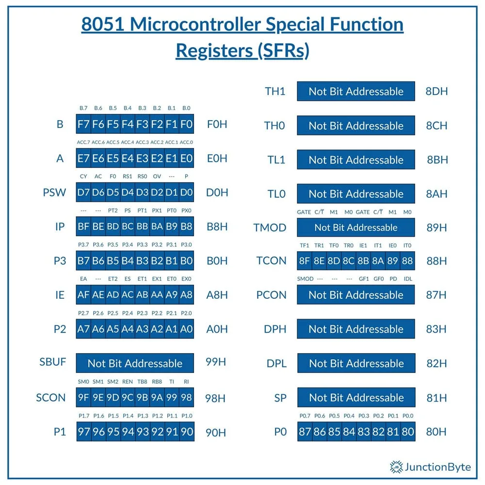
List of 8051 Microcontroller Special Function Registers (SFRs)
The following table lists out all the 21 8051 Microcontroller Special Function Registers (SFR). It also shows the internal RAM address of the SFR along with their bit-addressability status.
| Direct Address (Internal RAM) | SFR | Description | Bit Addressable |
| 80H | P0 | Port 0 Latch | Yes |
| 81H | SP | Stack Pointer | — |
| 82H | DPL | Data Pointer Higher Byte | — |
| 83H | DPH | Data Pointer Lower Byte | — |
| 87H | PCON | Power Control | — |
| 88H | TCON | Timer/Counter Control | Yes |
| 89H | TMOD | Timer/Counter Mode | — |
| 8AH | TL0 | Timer/Counter 0 Lower Byte | — |
| 8BH | TL1 | Timer/Counter 1 Lower Byte | — |
| 8CH | TH0 | Timer/Counter 0 Higher Byte | — |
| 8DH | TH1 | Timer/Counter 1 Higher Byte | — |
| 90H | P1 | Port 1 Latch | Yes |
| 98H | SCON | Serial Port Control | Yes |
| 99H | SBUF | Serial Port Data Buffer | — |
| A0H | P2 | Port 2 Latch | Yes |
| A8H | IE | Interrupt Enable | Yes |
| B0H | P3 | Port 3 Latch | Yes |
| B8H | IP | Interrupt Priority | Yes |
| D0H | PSW | Program Status Word | Yes |
| E0H | A | Accumulator | Yes |
| F0H | B | B Register | Yes |
If you write Assembly language programs for 8051 Microcontroller, then you need to know that you can either use the register name or the Address for some opcodes. For instance, you can use the name ‘A’ for the accumulator or the address 0E0H.
Notice the preceding ‘0’ when I mentioned the Address of the accumulator. That is because all addresses must start with a digit (any number).
Another interesting fact is that the binary address of all bit-addressable SFRs will be in the form of xxxxx000B.
Further, we can categorize these 21 registers into the following six groups:
| CPU Registers | A, B |
| Status Register | PSW |
| Pointer Registers | DPL, DPH, SP |
| I/O Port Latch Registers | P0, P1, P2, P3 |
| Peripheral Control Registers | PCON, SCON, TCON, TMOD, IE, IP |
| Peripheral Data Registers | TL0, TH0, TL1, TH1, SBUF |
Reset Value of 8051 Microcontroller SFRs
When the 8051 Microcontroller Resets (manual or power-on), the values of the SFRs will not be the same (prior to the reset). The following table shows the reset values of all the 8051 Microcontroller Special Function Registers.
| SFR | Reset Value (B) | Notes |
| A | 00000000 | |
| B | 00000000 | |
| DPTR (DPH DPL) | 00000000 00000000 | |
| IE | 0XX00000 | All Interrupts Disabled |
| IP | XXX00000 | |
| P0, P1, P2, P3 | 11111111 | Outputs FFH, All are INPUTs |
| PC | 00000000 00000000 | Address of First Instruction. Not an SFR but an important register. |
| PCON | 0XXXXXXX | Default Baud Rate Set by Timer 1 |
| PSW | 00000000 | |
| SBUF | XXXXXXXX | |
| SCON | 00000000 | |
| SP | 00000111 | 07H – Stack Starts from 08H |
| TCON | 00000000 | |
| TH0, TH1, TL0, TL1 | 00000000 | |
| TMOD | 00000000 |
8051 Microcontroller Special Function Registers
Accumulator (A or ACC)
The Accumulator (ACC or simply the A Register) is one of the most widely used registers of an 8051 Microcontroller (not only in terms of SFRs but overall registers). There are several instructions of the 8051 Microcontroller that directly use the A register as one of its operands.

This register stores or ‘accumulates’ the results of most arithmetic and logical operations of the ALU. Hence the name Accumulator. If the operation requires transfer of data between two registers, the data must go through the A Register.
The following a small list of operations that use the A register:
- Almost all Arithmetic Operations (Addition, Subtraction, Multiplication, Division)
- Most of the Logical Operations (AND, OR, NOT, EX-OR, Rotate)
- Any Data Transfer Operations between the 8051 Microcontroller and External Memory
In the SFR region, the address of the A register is E0H. It is both byte addressable and bit addressable. The individual bit addresses of the Accumulator are: E0H (Bit 0) to E7H (Bit 7).
If you notice, the Byte Address of the Accumulator and the Bit Address of the LSB (Bit 0) is the same i.e., E0H. The type of instruction differentiates whether we are accessing the full byte or only the Bit 0.
B Register
The B Register is another ‘CPU’ register that works closely with the ALU. Its primary usage is in Multiplication and Division operations. An interesting point about the 8051 Microcontroller is that both these Arithmetic Operations operate exclusively on A and B Registers.

During multiplication, the B Register holds one of the operands (multiplier or multiplicand). After the multiplication operation, the B Register holds the higher byte of the result.
We will take a closer look at the 8051 Microcontroller Instruction Set in a separate guide but for the time being, the multiplication instruction is as follows:
- MUL AB
This instruction multiplies the Accumulator with the data in the B Register and puts the 16-bit result in B (higher byte of the result) and A (lower byte of the result) registers.
In case of division operation, the B Register holds the divisor. After the division operation, the B Register holds the remainder (while the Accumulator contains the Quotient).
- DIV AB
- ; A = INT[A/B]
- ; B = MOD[A/B]
Apart from multiplication and division, we can also use the B Register as a General Purpose Register using its byte address F0H (or individual bit addresses F0H to F7H).
PSW (Program Status Word)
The Program Status Word or PSW is an important SFR. in the MCS-51 (8051) Architecture. This register contains several ‘Flags’ that reflect the status of operation performed by the CPU.
If you aren’t familiar, a ‘Flag’ is a 1-bit storage element that is automatically SET (‘1’) or RESET (‘0’) depending on the result of the arithmetic or logical operation performed by the CPU.
In case of the PSW, it contains the following flag bits: Carry Flag, Auxiliary Carry Flag, User Programmable Flag, Overflow Flag, and Parity Bit.
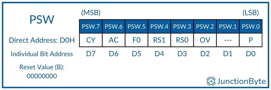
Instructions use these flags as reference to make essential decisions (branching or program flow control).
Apart from these Flags, the PSW also contains two bits that help us set the active Register Bank.
The address of the PSW Register is D0H. As it is a bit-addressable register, you can assess its individual bits from the addresses D0H to D7H.
Here is the structure of the PSW register with its elements and addresses.
The following table gives a brief summary of the bits of the PSW register:
| Bit | Symbol | Direct Bit Address (Alternate Address) | Bit Function |
| 7 | CY | D7H (PSW.7) | Carry Flag. Used in Arithmetic, Logical, and Boolean Operations |
| 6 | AC | D6H (PSW.6) | Auxiliary Carry Flag. Used exclusively in BCD Arithmetic Operations |
| 5 | F0 | D5H (PSW.5) | Flag 0. General Purpose User Programmable Flag |
| 4 | RS1 | D4H (PSW.4) | Register Bank Selection Bit 1. |
| 3 | RS2 | D3H (PSW.3) | Register Bank Selection Bit 0. |
| 2 | OV | D2H (PSW.2) | Overflow Flag. Used in Arithmetic Operations |
| 1 | — | D1H (PSW.1) | Reserved. May be used as a General Purpose USer Programmable Flag |
| 0 | P | D0H (PSW.0) | Parity Bit. Set or Reset depending on the number of ones in the A Register |
Let me explain all these bits of the PSW register.
Carry Flag
The Carry Flag (CY) is ‘Set’ if there is a carry out from the MSB (Bit 7) after addition. During subtraction, this flag is set if there is a borrow into the Bit 7. Otherwise, the Carry Flag is reset.
Additionally, the Carry Flag also acts as a Boolean Accumulator. It serves as a ‘1-bit register’ for boolean instructions.
Auxiliary Carry Flag
The Auxiliary Carry (AC) is similar to the regular Carry Flag except that it works exclusively for BCD (Binary-Coded-Decimal) values. This flag will be set if there is a carry out from bit 3 into bit 4.
F0 (Flag 0)
It is a general-purpose flag and the CPU of the 8051 Microcontroller doesn’t use it. We can use this flag in applications as a 1-bit memory storage (to record or trigger an event).
Register Bank Selection Bits (RS0 and RS1)
If you remember the 8051 Microcontroller Memory Organization, especially the Data Memory, the lower 128 Bytes of the RAM is an interesting region. In that, the first 32 Bytes are grouped into four Register Banks, each with eight registers.
Only one of the four register banks can be active at any time and these bits in the PSW register help in selecting the active register bank.
The following table shows the combination of the RS0 and RS1 bits and their corresponding Register Banks.
| RS1 | RS0 | Register Bank | Register Address in RAM |
| 0 | 0 | Bank 0 | R0 – R7 -> 00H -07H |
| 0 | 1 | Bank 1 | R0 – R7 -> 08H -0FH |
| 1 | 0 | Bank 2 | R0 – R7 -> 10H -17H |
| 1 | 1 | Bank 3 | R0 – R7 -> 18H -1FH |
We can SET or RESET the values of the RS0 and RS1 bits of the PSW Register in our applications and set the active Register Bank.
Overflow Flag
If the result of an arithmetic operation (addition or subtraction) goes out of range, then the Overflow Flag is set (‘1’). This usually happens when we perform arithmetic operations on two signed numbers. If the result is greater than +127 or less than -128, then the Overflow Flag will be set.
In case of unsigned numbers, we can ignore the Overflow Flag.
Parity Bit
After each machine cycle, the Parity Bit is automatically ‘Set’ or ‘Reset’ by counting the number of 1’s in the Accumulator. If the Accumulator has an even number of ones, the Parity Bit will be Reset (0), otherwise, it will be set (1).
The combined Parity of the Accumulator and the Parity Bit should always be even.
DPTR (Data Pointer)
Almost all the Registers that we have seen till now are 8-bit wide. The Data Pointer or DPTR is a 16-bit register that is a combination of two 8-bit registers DPL and DPH. Here, the DPL and DPH are the lower and higher bytes of the DPTR register.
Physically, the DPTR register doesn’t have a dedicated memory space. However, the DPL and DPH registers have separate addresses in the SFR region of the RAM (DPL — 82H and DPH — 83H).
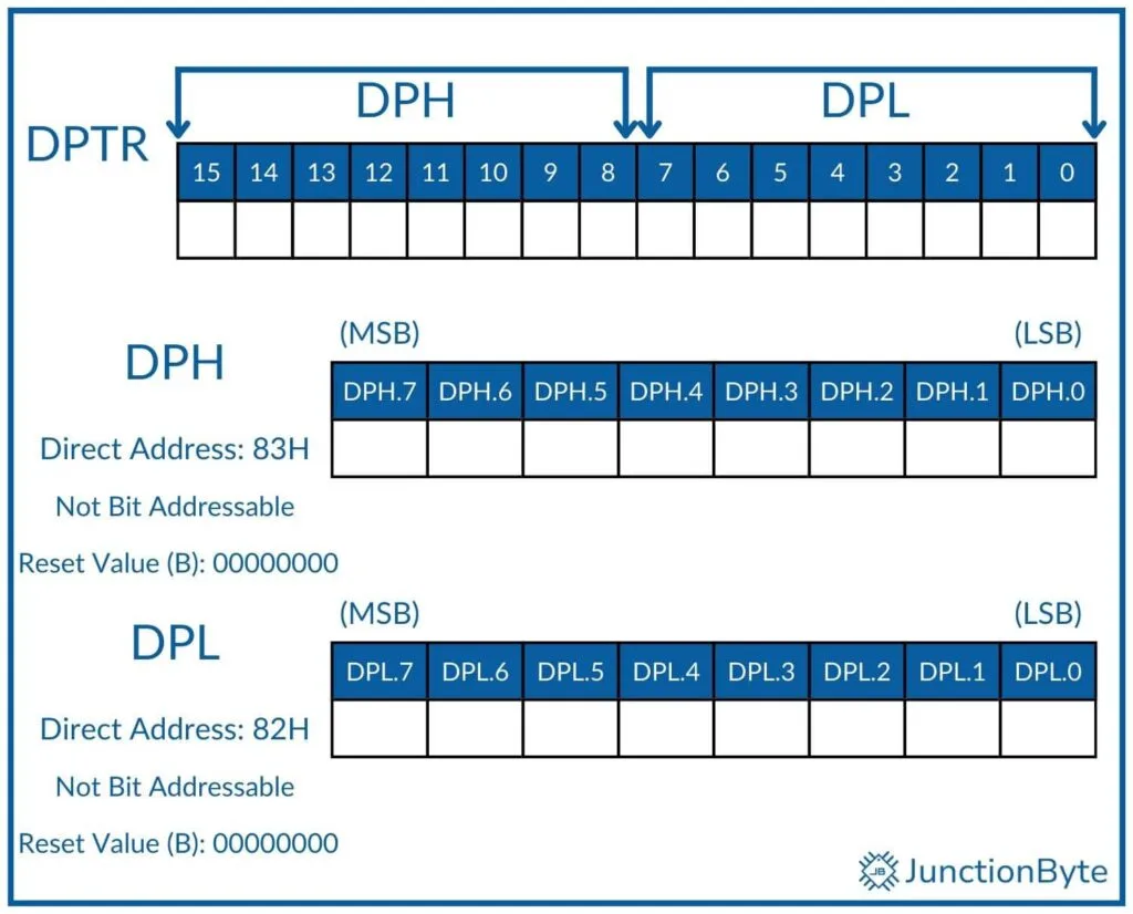
We can either access the individual registers (DPL or DPH) or the DPTR as a single 16-bit register. When we use DPTR in our program, we are indirectly using the DPL and DPH registers.
Coming to the applications, the DPTR register is used when accessing external program (ROM) or data (RAM) memories (or even internal ROM). It always contains the 16-bit address of the external memory.
For example, if you want to write the data ‘69H’ to an external RAM address of ‘1010H,’ here are the instructions you need to implement.
MOV A, #69H ; load 69H to Accumulator using immediate addressing
MOV DPTR, #1010H ; load the 16-bit address constant to DPTR using
; immediate addressing
MOV @DPTR, A ; move value in A (69H) to address pointed by DPTR
; using indirect addressing
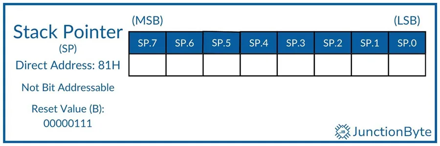
SP (Stack Pointer)
Stack is a region in RAM that works with a bunch of special instructions (opcodes) to store and retrieve data. These instructions include: PUSH, POP, CALL, and RET. Stack memory comes into play during subroutine/function calls.
Coming to the Stack Pointer (SP), it is an 8-bit register that holds the address of the ‘top of the stack.’ If we want to write data to the Stack (using PUSH instruction), then the value in Stack Pointer increases by one (SP = SP + 1) and the data is then written to this new address.
Similarly, when we retrieve data from the Stack (using POP), the opposite happens. It will provide data at the location pointed by the Stack Pointer and then the value of the SP is decremented by one (SP = SP – 1).
The address of the SP register in the SFR Address Space is 81H. After system reset, the value of the SP becomes 07H. So, if we perform a PUSH operation after reset, then the data will be written at 08H. Note that the address in the SP after reset (07H) collides with the R7 register of Register Bank 0. If we do not reinitialize the SP, then the Register Banks 1, 2, and 3 may not be available (as Stack Memory uses that region of RAM).
In 8051 Microcontrollers, the Stack Memory is often restricted to Internal RAM that supports Indirect Addressing Mode. This means, you can technically use the entire 256 Bytes of Internal RAM of a typical 8052 Microcontroller. This includes the lower 128 Byte region (accessible through direct and indirect addressing) and the upper 128 Byte region (accessible through indirect addressing only).
A good practice is to use the upper 128 Bytes of the RAM as Stack Memory since it supports only indirect addressing and you won’t lose access to Register Banks and Bit Addressable regions.
P0, P1, P2, P3 — I/O Port Registers (Latches)
Almost all the interactions between the 8051 Microcontroller and the external world happens through the four I/O Ports. Whether you want to add external memories (Program or Data) or interface any I/O devices (sensors, input, display, etc.), all this communication is possible only through the I/O Ports.
Each I/O Port has a dedicated SFR in the RAM. The following list shows the four I/O Port Registers and their corresponding addresses:
- P0 — 80H
- P1 — 90H
- P1 — A0H
- P2 — B0H
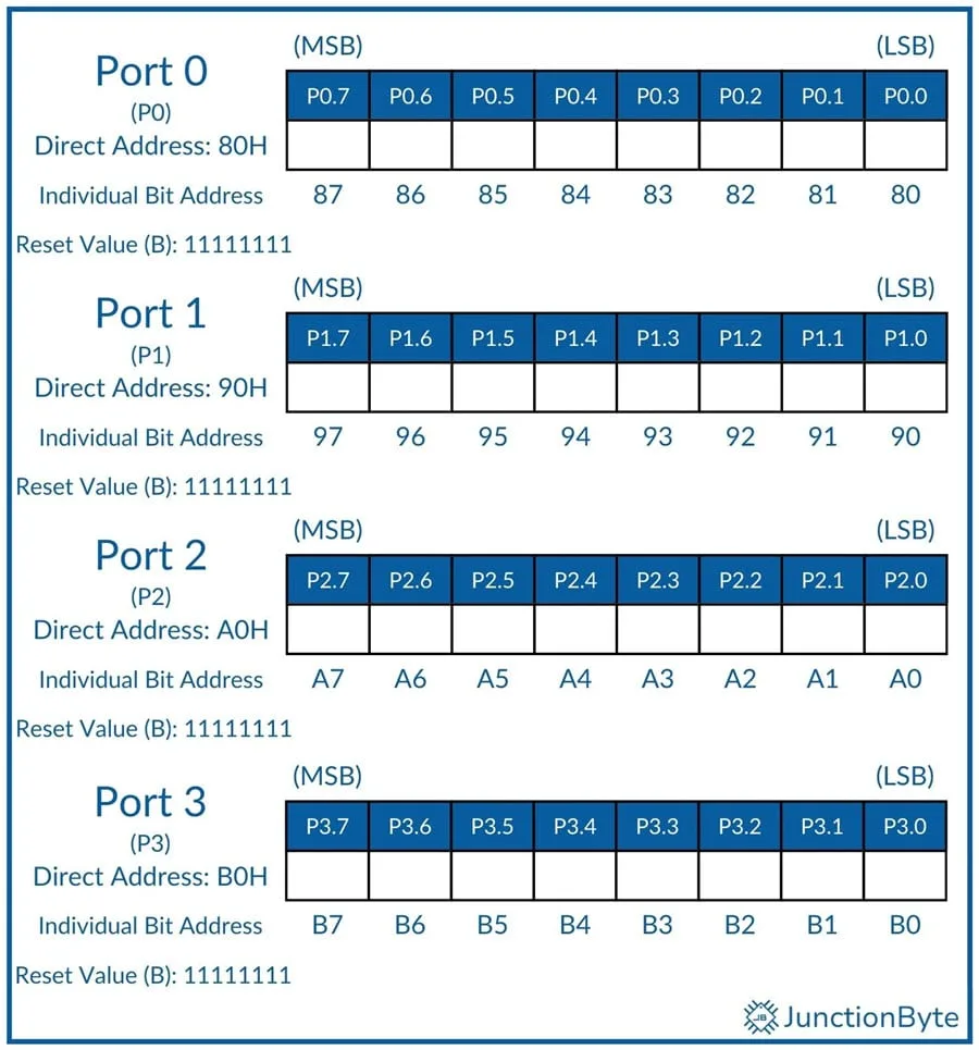
Each Bit in these SFRs is associated with the respective physical Pin of the I/O Port. For example, Bit 1 of SFR P1 corresponds to Pin P1.1.
So, if we Set or Reset a bit in one of these SFRs, then it translates to VCC or 0V on the respective physical pin. We are essentially using the Pins as Output to drive loads (LEDs or Motors). To use these Ports as Outputs, we have to write data to the Port SFRs.
To make a particular I/O as Input, we have to write logic ‘1’ to the respective bit of the SFR. After reset, all the four Port Registers have values FFH (which means they act as Inputs after reset). If there is any incoming data, it will be written to the Port Register. So, to read input data from these ports, we have to read the Port SFRs.
These four SFRs are both byte and bit addressable. Also, Ports 0, 2, and 3 have dual functions.
PCON (Power Control)
Located at the address 87H in the SFR Memory Space, the PCON or Power Control Register contains special bits for configuring the power mode of the 8051 Microcontroller. Despite that, the PCON register is not bit-addressable.
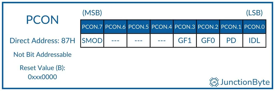
The following table shows the summary of the bits of PCON Register:
| Bit | Symbol | Description |
| 7 | SMOD | Serial Baud-Rate Modify Bit |
| 6 — 4 | — | Undefined / Not implemented |
| 3 | GF1 | General Purpose User Flag Bit 1 |
| 2 | GF0 | General Purpose User Flag Bit 0 |
| 1 | PD | Power Down Bit |
| 0 | IDL | Idle Mode Bit |
SMOD
When Timer 1 is used to generate the baud rate for Serial Communication (UART), we can double the Baud Rate by setting this bit (making it 1). This is applicable to Serial Modes 1, 2, or 3.
If we clear this bit (make it 0, which is also the state after reset), then Serial Communication uses baud rate set by Timer 1.
GF0 and GF1
These two bits are user programmable general purpose flag bits. The application can set or clear these bits and use them as reference in the program.
IDL (Idle Mode)
During normal operation, the internal clock circuit provides the clock signal to all the different peripherals of the Microcontroller. However, if we set the IDL Bit (PCON.0) as 1, the 8051 Microcontroller enters Idle Mode.
In this mode, the clock circuit stops providing clock to the CPU but continues to provide clock for all the other peripherals (Timer/Counters, Serial, I/O Ports, Interrupts).
This means the CPU will not fetch and execute any instructions in Idle Mode. As a result, the power consumption drops significantly (draws only 5 to 6 mA). As far as the remaining peripherals are concerned, the I/O Ports output data as normal (the data that is latched in their registers before CPU enters Idle Mode). The contents of the RAM and SFR remain the same.
To come out of Idle Mode, we have to use the Reset or any interrupt that is already enabled prior to entering Idle Mode.
PD (Power Down)
When we set the PD Bit (PCON.1) of the PCON SFR as 1, then the 8051 Microcontroller enters a Power Down Mode. In this mode, all the peripherals, including the CPU, stop receiving the clock signal. Only the I/O Ports, RAM and ROM will be active.
In this mode, the power consumption is significantly less (draws around 100µA). In the original 8051 Microcontroller, the only way to come out of the Power Down Mode is to apply a hardware reset.
However, some modern 8051 Microcontrollers (including the AT89S52) can exit Power Down Mode from External Interrupts that are already enabled.
I will talk more about 8051 Microcontroller Power Down and Idles Modes in a separate guide with practical examples.
SCON (Serial Port Control)
We have to use the SCON Register to configure the Serial Port of the 8051 Microcontroller. It is located at the address 98H in the SFR Memory Space. The SCON Register is both Byte and Bit Addressable.
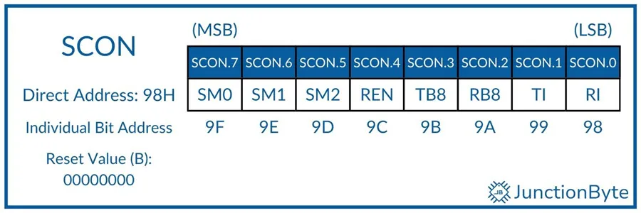
Speaking of Bits, the following table shows a brief description of all the bits of the SCON SFR.
| Bit | Symbol | Description |
| 7 | SM0 | Serial Port Mode Selection Bit 0 |
| 6 | SM1 | Serial Port Mode Selection Bit 1 |
| 5 | SM2 | Serial Port Mode Selection Bit 2. Enable Multiprocessor Communication Feature |
| 4 | REN | Enable Serial Reception |
| 3 | TB8 | Transmit Bit 8. The 9th Bit that will be transmitted in Modes 2 and 3 |
| 2 | RB8 | Receive Bit 8. The 9th Bit that is received in Modes 2 and 3 |
| 1 | TI | Transmit Interrupt Flag. Set by hardware at the end of Transmission. |
| 0 | RI | Receive Interrupt Flag. Set by hardware at the end of Reception. |
SM0 and SM1
The SM0 and SM1 bits specify the Serial Port Mode of the 8051 Microcontroller as follows:
| SM0 | SM1 | Mode | Description | Baud Rate |
| 0 | 0 | 0 | 8-Bit Synchronous Shift Register Mode | Fixed Baud Rate (Baud Rate = FOSC/12) |
| 0 | 1 | 1 | Standard 8-Bit UART Mode | Variable Baud Rate (Can be set by Timer) |
| 1 | 0 | 2 | 9-Bit UART Mode (support for Multiprocessor Communication) | Fixed Baud Rate (Baud Rate = FOSC/32 or FOSC/64) |
| 1 | 1 | 3 | 9-Bit UART Mode (support for Multiprocessor Communication) | Variable Baud Rate (Can be set by Timer) |
I will explain in detail about the different Serial Communication Modes in a separate 8051 Microcontroller Serial Guide.
TCON (Timer/Counter Control)
The Timer Control TCON Register consists of status and control bits for both the Timers (Timer 0 and Timer 1). It is a bit addressable register and is located at the address 88H in SFR Memory Space.
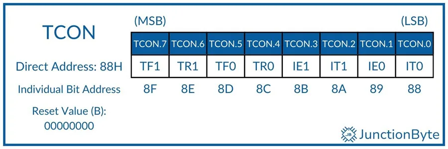
The lower four bits in the TCON register are associated with External Interrupts and have nothing to do with Timers or Counters. Coming to the upper four bits, they are used to enable/disable the timers as well as contain the overflow flags.
| Bit | Symbol | Description | Notes |
| 7 | TF1 | Timer 1 Overflow Flag | Set by hardware when Timer/Counter 1 Overflows. Cleared by hardware when the CPU executes an ISR at 001BH. |
| 6 | TR1 | Timer 1 Run Control Bit | Set or Clear to turn Timer/Counter 0 ON or OFF. |
| 5 | TF0 | Timer 0 Overflow Flag | Set by hardware when Timer/Counter 1 Overflows. Cleared by hardware when the CPU executes an ISR at 000BH. |
| 4 | TR0 | Timer 0 Run Control Bit | Set or Clear to turn Timer/Counter 0 ON or OFF. |
| 3 | IE1 | Interrupt 1 Edge Flag | Set by hardware when it detects an external interrupt edge (HIGH to LOW on INT1 – P3.3). Cleared by hardware when CPU executes Interrupt 1 ISR (at 0013H). |
| 2 | IT1 | Interrupt 1 Type Control Bit | If 1, INT1 is a Falling Edge Triggered Interrupt. If 0, INT1 is a Low-level Triggered Interrupt. |
| 1 | IE0 | Interrupt 0 Edge Flag | Set by hardware when it detects an external interrupt edge (HIGH to LOW on INT0 – P3.2). Cleared by hardware when CPU executes Interrupt 0 ISR (at 0003H). |
| 0 | IT0 | Interrupt 0 Type Control Bit | If 1, INT0 is a Falling Edge Triggered Interrupt. If 0, INT0 is a Low-level Triggered Interrupt. |
TMOD (Timer/Counter Mode Control)
The Timer/Counter Mode Control Register or TMOD is a special function register that helps in selecting the mode of the Timers 0 and 1. The lower four bits control Timer 0 while the higher four bits control Timer 1. First, we will look at the different bits in the TMOD register and later I will explain the meaning of these bits in detail.

The TMOD register is located at the address 89H in the SFR Memory Space and is not bit addressable.
| Bit | Symbol | Description |
| 7 | GATE | OR Gate Enable Bit for Timer 1 |
| 6 | C/T | Set Timer 1 as Counter or Timer |
| 5 | M1 | Timer/Counter Operating Mode Select Bit 1 for Timer 1 |
| 4 | M0 | Timer/Counter Operating Mode Select Bit 0 for Timer 1 |
| 3 | GATE | OR Gate Enable Bit for Timer 0 |
| 2 | C/T | Set Timer 0 as Counter or Timer |
| 1 | M1 | Timer/Counter Operating Mode Select Bit 1 for Timer 0 |
| 0 | M0 | Timer/Counter Operating Mode Select Bit 0 for Timer 0 |
The naming can be confusing. So, for the sake of understanding and easy explanation, I will use the following naming convention.
| Bit 7 — GATE —> GATE1 |
| Bit 6 — C/T —> C/T1 |
| Bit 5 — M1 —> T1M1 |
| Bit 4 — M0 —> T1M0 |
| Bit 3 — GATE —> GATE0 |
| Bit 2 — C/T —> C/T0 |
| Bit 1 — M1 —> T0M1 |
| Bit 0 — M0 —> T0M0 |
GATE
The GATE bit in the TMOD Register determines whether the Timer/Counter is either software controlled or hardware controlled.
In the case of Software Control, only the Timer Run Control Bit in the TCON register is sufficient to start or stop the corresponding timer/counter operation.
Coming to Hardware Control, in addition to the Timer Run Control Bit, the External Interrupt Pin also determines the Timer/Counter Start/Stop state.
| GATE0 | 0 | Timer/Counter 0 is enabled when TR0 in TCON is 1 |
| 1 | Timer/Counter 0 is enabled when TR0 in TCON is 1 and INT0 Pin is HIGH | |
| GATE1 | 0 | Timer/Counter 1 is enabled when TR1 in TCON is 1 |
| 1 | Timer/Counter 1 is enabled when TR1 in TCON is 1 and INT1 Pin is HIGH |
C/T
The C/T bit of the TMOD Register sets the Counter or Timer operation of the respective module.
| C/T0 | 0 | Timer/Counter 0 acts as Timer and counts the internal frequency (from the internal oscillator) |
| 1 | Timer/Counter 0 acts as Counter and counts the pulses from external input on pin P3.4 (T0) | |
| C/T1 | 0 | Timer/Counter 1 acts as Timer and counts the internal frequency (from the internal oscillator) |
| 1 | Timer/Counter 1 acts as Counter and counts the pulses from external input on pin P3.5 (T1) |
M0 and M1
The M0 and M1 bits of the TMOD Register set the Timer Mode. Timers in 8051 Microcontrollers have four modes of operation. Both the Timers (Timer 0 and Timer 1) have the same set of operating modes.
| M1 | M0 | Mode | Description |
| 0 | 0 | 0 | 13-Bit Timer Mode (THx is 8-Bit Timer with TLx as 5-bit Prescaler) |
| 0 | 1 | 1 | 16-Bit Timer Mode (THx and TLx are cascaded, no prescaler) |
| 1 | 0 | 2 | 8-Bit Auto-reload Timer/Counter (when TLx overflows, it is loaded with value in THx) |
| 1 | 1 | 3 | Split Timer Mode (two 8-Bit Timers). TL0 and TH0 are two timers/counters that are controlled by Timer 0 and Timer 1 control bits. Timer 1 is disabled. |
NOTE: x = 0 for Timer 0 and x = 1 for Timer 1
IE (Interrupt Enable)
An important SFR in the 8051 Microcontroller is the Interrupt Enable or IE Register. Using this register, you can enable or disable interrupts. The original 8051 Microcontroller has support for five interrupt sources: two external, Timers (0 and 1), and Serial. The 8052 variant adds Timer 2 as another interrupt source.
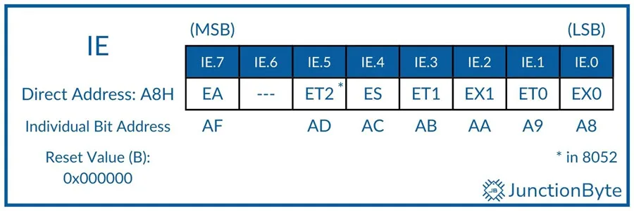
In the 8051 Microcontroller SFR Address Space, the IE register is located at A8H and it is bit addressable.
| Bit | Symbol | Description | Notes |
| 7 | EA | Global Interrupt Enable/Disable Bit | EA=0, all Interrupts are disabled.EA=1, individual interrupts can be enabled/disabled |
| 6 | — | Reserved | |
| 5 | ET2 | Reserved in original 8051. Timer 2 Overflow Interrupt Enable Bit | ET2=0, Timer 2 Overflow Interrupt is Disabled.ET2=1, Timer 2 Overflow Interrupt is Enabled. |
| 4 | ES | Serial Port Interrupt Enable Bit | ES=0, Disable Serial Port Interrupt (TI or RI).ES=1, Enable Serial Port Interrupt (TI or RI). |
| 3 | ET1 | Timer 1 Overflow Interrupt Enable Bit | ET1=0, Timer 1 Overflow Interrupt is Disabled.ET1=1, Timer 1 Overflow Interrupt is Enabled. |
| 2 | EX1 | External Interrupt 1 Interrupt Enable Bit | EX1=0, Disable External Interrupt 1.EX1=1, Enable External Interrupt 1. |
| 1 | ET0 | Timer 0 Overflow Interrupt Enable Bit | ET0=0, Timer 0 Overflow Interrupt is Disabled.ET0=1, Timer 0 Overflow Interrupt is Enabled. |
| 0 | EX0 | External Interrupt 0 Interrupt Enable Bit | EX0=0, Disable External Interrupt 0.EX0=1, Enable External Interrupt 0. |
IP (Interrupt Priority)
Another ‘interrupt-related’ SFR in 8051 Microcontroller is the Interrupt Priority or IP Register. It is located at B8H address in the SFR Memory Space and is bit addressable. Using the IP register, we can set the priority of a particular interrupt as high or low. When a bit in the IP register is set as 1, then it assigns a high priority to the corresponding interrupt. In case the bit is cleared, then it assigns a low priority.
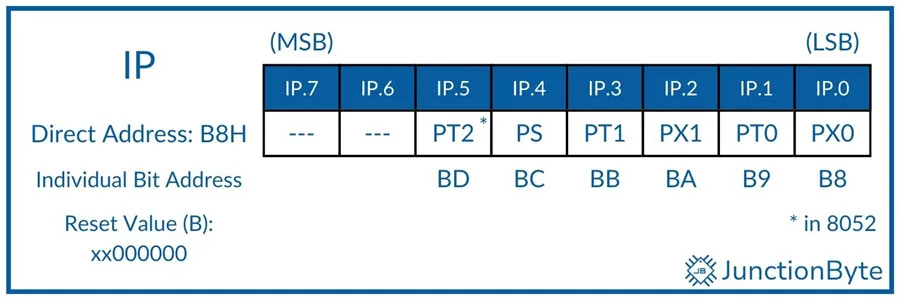
| Bit | Symbol | Description |
| 7 | — | Reserved |
| 6 | — | Reserved |
| 5 | PT2 | Reserved in original 8051. Timer 2 Interrupt Priority Bit |
| 4 | PS | Serial Port Interrupt Priority Bit |
| 3 | PT1 | Timer 1 Interrupt Priority Bit |
| 2 | PX1 | External Interrupt 1 Interrupt Priority Bit |
| 1 | PT0 | Timer 0 Interrupt Priority Bit |
| 0 | PX0 | External Interrupt 0 Interrupt Priority Bit |
If we set two sources of interrupts as high priority, then the interrupt handling mechanism uses the following sequence to determine which interrupts gets precedence:
- External Interrupt 0 ——— Highest Priority
- Timer 0 Overflow Interrupt
- External Interrupt 1
- Timer 1 Overflow Interrupt
- Serial Port Interrupt
- * Timer 2 Overflow Interrupt ——— Lowest Priority
* Not in the original 8051.
SBUF (Serial Data Buffer)
The next set SFRs are not that special as they are essentially a bunch of data storing registers specific to their peripheral. First, we have the SBUF or Serial Data Buffer Register located at the address 99H. It is an 8-bit register that holds the serial data during serial transmission and receptions.
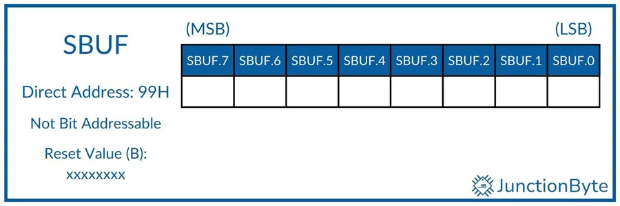
If you want to send a Byte of data through the TXD Pin of the Serial Port, then you have to write that data into the SBUF register. Similarly, when you receive a Byte of data through the RXD pin, the data is stored in the SBUF registers and we can read from it.
TL0/TH0 (Timer 0 Registers Low/High)
The job of Timers in 8051 Microcontroller is to basically count the internal clock pulses (Timer) or external pulses (Counter). Each Timer consists of two 8-bit registers that hold the count. In the case of Timer 0, it has TL0 and TH0 registers that act as low and high bytes of the timer/counter. Their addresses are TL0 – 8AH and TH0 – 8CH and they are not bit addressable.
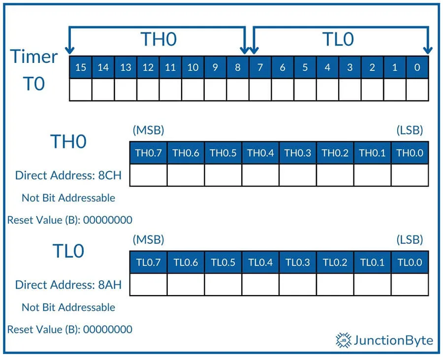
Together, they form a 16-Bit register that can count up to 65,535. For example, if the value of Timer 0 is 6969 (decimal), then contents of TL0 and TH0 are as follows:
- 6969 -> 1B39H
- TH0 -> 1BH
- TL0 ->39H
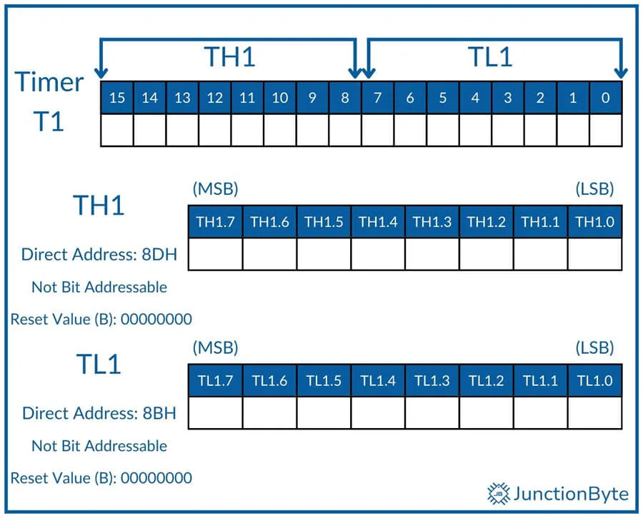
TL1/TH1 (Timer 1 Registers Low/High)
The above discussion on Timer 0 registers applies here as well. TL1 and TH1 are the low and high byte registers of Timer 1 located at 8BH and 8DH respectively.
Conclusion
A complete and in-detailed guide on 8051 Microcontroller Special Function Registers (SFRs). I discussed all the 8051 SFRs along with their bits (content structure), address, whether they are bit addressable or not, as well as the reset values.
As we further explore the 8051 Microcontroller, I will explain how these SFRs help us in configuring the microcontroller as per our needs.