One of the main differences between a Microprocessor and a Microcontroller is that the latter contains both the program and data memories right on the chip. This is also true for the 8051 Microcontroller as it has both ROM (usually Flash or EEPROM) and RAM on the same die as the CPU. If you want a deeper understanding of the 8051 Microcontroller Architecture, you need to learn the 8051 Microcontroller Memory Organization.
In this guide, I will talk about the memory layout of the 8051 Microcontroller and how the CPU inside the 8051 will access both the program and data memories. In addition to this, we will also learn how to interface external memory with the 8051 Microcontroller.
Before proceeding, I would recommend you to go through the previous guides on the 8051 Microcontroller: Introduction to 8051 Microcontroller, 8051 Microcontroller Pin Diagram, and 8051 Microcontroller Architecture. This guide will be a continuation of the previous ones.
Recap of Microcontroller Memory Architecture
In the previous guide (8051 Microcontroller Architecture), we learned that there are two types of Microcontroller Architectures based on how the CPU accesses the memories. They are:
- von Neumann Architecture
- Harvard Architecture
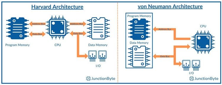
In von Neumann Architecture, both the Program (Instructions) and Data are on the same memory storage unit. The CPU can access either instructions or data at any given time.
Coming to the Harvard Architecture, it has separate memories for storing program and data.
Almost all modern microcontrollers (apart from a few odd ones) use the Harvard Architecture and that includes the 8051 Microcontroller.
8051 Microcontroller Memory Organization
Even though both the program and data memory of the 8051 Microcontroller reside on the same die, they are logically and physically separate. The address space for accessing these memories is also separate.
The Program Memory is where we store the code (all the instructions). The CPU can only read from the Program Memory.
When the CPU in the Microcontroller is executing instructions, it must store the data somewhere that is easily accessible (CPU should be able to read and write data). In addition to data, there will be a lot of temporary results while performing arithmetic computations.
The Data Memory of a Microcontroller acts as this temporary storage where the CPU can keep all the data and temporary results.
The original 8051 Microcontroller had 4K Bytes of on-chip Program Memory (ROM) and 128 Bytes of Data Memory (RAM). Later versions of the 8051 Microcontroller (for instance, the AT89S52) came with 8K Bytes of Program Memory (Flash) and 256 Bytes of Data Memory (RAM).
Alternatively, the 8051 Microcontroller can access up to 64K Bytes of External Program and Data Memories each.
For the sake of an easy explanation of the 8051 Microcontroller Memory Organization, I will use the AT89S52 as a reference for all the numbers. You can apply similar methods to understand the memory organization of any 8051-based Microcontroller.
Program (Code) Memory
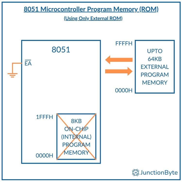
As I mentioned in the previous section, the 8051 Microcontroller has 8KB of on-chip Program Memory. With 8KB of Memory, the Address Space becomes 0000H to 1FFFH.
If you connect the EA (External Access) pin to VCC (HIGH or Logic 1), then all the fetches for the program within the addresses 0000H through 1FFFH will happen from the Internal Memory.

In case you connected an external program memory to the 8051 Microcontroller and want to use it in conjunction with the internal memory, then it is possible with the EA pin pulled HIGH. For the first 8K Addresses (0000H to 1FFFH), the CPU will fetch the program from the Internal Program Memory. For any addresses beyond this range i.e., 2000H to FFFFH, CPU will fetch instructions from the External Memory.
If we connect the EA pin to GND (LOW or Logic 0), then the CPU will ignore the internal program memory altogether and only fetches instructions from the External Program Memory. In this case, the complete address range of 0000H to FFFFH is accessed from the external program memory.
Data Memory
Coming to the Data Memory, the 8051 Microcontroller has 256B of on-chip Data Memory. We can divide this into the lower 128 Bytes (in the address range 00H to 7FH) and upper 128 Bytes (in the address range of 80H to FFH).
The lower 128 Bytes is further divided into three regions:
- First 32 Bytes (00H to 1FH): Four Register Banks; each with eight 8-bit Registers
- Next 16 Bytes (20H to 2FH): Bit and Byte Addressable Data Memory
- Last 80 Bytes (30H to 7FH): 80 Byte-Addressable General Purpose Registers
The upper 128 Bytes (80H to FFH) act as additional general purpose memory (byte addressable).

Now comes the interesting part. The Special Function Registers or SFRs also have the same address range as the upper 128 Bytes i.e., 80H to FFH. How is this possible?
Physically, the SFR Space is separate from the upper 128 Bytes of the Data Memory. However, the reason for sharing the same address space is the limitation of 8-bit addressing of the 8051 Microcontroller.
Internally, the 8051 uses an 8-bit Address Bus to access the Data Memory. With an 8-bit address, it can access only 28 memory locations i.e., only 256 locations.
So, SFRs share the address space with the upper 128 Bytes of the RAM. How will the CPU know whether it is accessing general purpose memory or SFR?
This is where the Addressing Mode of the 8051 Microcontroller comes into play. When the address is above 7FH, the type of addressing mode will determine if the CPU accesses the upper 128B of RAM or SFR.
SFRs Address Space uses Direct Addressing Mode while the Upper 128B of RAM uses Indirect Addressing Mode.
Let us take a detailed-look at different sections of the Data Memory.
Register Banks
The first 32 Bytes of the Lower 128 Byte Section of the Internal Data Memory (RAM) consists of Register Banks. These 32 Bytes are divided into four Register Banks: Bank 0, Bank 1, Bank 2, and Bank 3.
Further, each ‘Bank’ consists of eight 8-bit registers, called R0, R1, R2, R3, R4, R5, R6, and R7. Each ‘Bank’ has a separate address range:
- Bank 0 — 00H to 07H
- Bank 1 — 08H to 0FH
- Bank 2 — 10H to 17H
- Bank 3 — 18H to 1FH
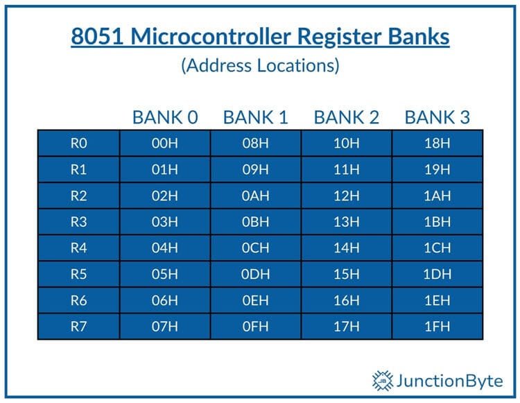
When we say ‘R4’ of Bank 0, then it means memory location 04H. Similarly, if we say ‘R4’ of Bank 2, then the address is 14H.
Only one ‘Bank’ can be active at any time and the registers R0, R1, etc. will correspond to that ‘Bank’ only. So, the names R0, R1, etc. will be the same but depending on the active Bank, the address will vary. There is an SFR known as PSW (Processor Status Word) that helps in selecting the Bank (using its bits RS0 and RS1).
Instead of using the Register names, you can use the addresses (for example, 00H instead of R0 of Bank 0) and it will act as a general purpose RAM.
However, there is an advantage of using Register names, thanks to the ‘Register Addressing Mode.’ If an instruction uses these Register names, they will occupy less space and require less time for execution. More about Addressing Modes in a separate guide.
Bit-Addressable Memory
The addresses from 20H to 2FH of the on-chip Data Memory (RAM) are bit addressable (in addition to being byte addressable). It means, you can work on the individual bit (Set, Clear, etc.) of an address without impacting the remaining seven bits.
To make things easy, these bits have respective Bit Addresses from 00H to 7FH. In total, there are 128 addressable bits (16 Bytes with 8-bits each).
When you use Boolean Instructions (Single-bit Instructions) with these addresses, the CPU will understand that the addresses are not regular addresses but bit addresses of the RAM.
For example,
- MOV 21H, #00H ; Clear memory location 21H
- SETB 09H ; Store logic 1 in bit address 09H.
- MOV 21H, #0F4H ; Load memory location 21H with F4H
In the first instruction, all the bits of the Memory Location 21 are set to 0 (contents of address 21H – 00000000b). The second instruction will set the bit with address 09H. So, the contents of address 21H will become 00000010b.
The last bit will load 11110100b to the address 21H. This means the previous bit-operation is over-written. Must be very careful when using the combination of bit and byte addresses.
General Purpose RAM
In the lower 128 Bytes of the Data Memory, the addresses from 30H to 7FH is the general purpose RAM. We can use it to store all sorts of temporary data. These 80 Bytes are byte addressable though.
Additionally, the upper 128 Bytes (80H to FFH) also acts as general purpose RAM. However, as I mentioned before, you have to use Indirect Addressing for these upper 128B of memory. The lower 128 Bytes can have Direct or Indirect Addressing.
If your program uses ‘Stack,’ you can make use of the upper 128 Bytes of the RAM as stack operations use Indirect Addressing.
All this ‘general purpose’ RAM section is also known as Scratchpad RAM.
Special Function Registers (SFRs)
I will explain the 8051 Microcontroller Special Function Registers (SFRs) in a separate guide. For the time being, the address range of 80H to FFH is reserved for SFRs. Out of the 128 Bytes, we (users) have access to only 21 Bytes of memory address i.e., the 8051 Microcontroller has 21 SFRs.
What about the remaining 107 Bytes? Depending on the variant of the 8051 Microcontroller, these addresses are either assigned to other data such as the TMP1 and TMP2 Registers that we saw in the 8051 Microcontroller or reserved for a future implementation. You should not read or write any data from/to these addresses.
Coming to SFRs, these are special regions of the on-chip RAM that act as CPU Registers (ACC and B Register), Port Latches (P0, P1, etc.), Status and Control Bits, etc. They essentially control the on-chip peripherals.
Since these share the same address space as the upper 128 Bytes of the RAM, they use Direct Addressing to differentiate from the regular RAM.
Some of these registers are both byte and bit addressable (all registers are byte addressable).
The following table shows all the SFRs and their respective Addresses in the on-chip RAM.
| SFR | Description | Direct Address |
| P0 | Port 0 Latch | 80H |
| SP | Stack Pointer | 81H |
| DPL | Data Pointer Higher Byte | 82H |
| DPH | Data Pointer Lower Byte | 83H |
| PCON | Power Control | 87H |
| TCON | Timer/Counter Control | 88H |
| TMOD | Timer/Counter Mode | 89H |
| TL0 | Timer/Counter 0 Lower Byte | 8AH |
| TL1 | Timer/Counter 1 Lower Byte | 8BH |
| TH0 | Timer/Counter 0 Higher Byte | 8CH |
| TH1 | Timer/Counter 1 Higher Byte | 8DH |
| P1 | Port 1 Latch | 90H |
| SCON | Serial Port Control | 98H |
| SBUF | Serial Port Data Buffer | 99H |
| P2 | Port 2 Latch | A0H |
| IE | Interrupt Enable | A8H |
| P3 | Port 3 Latch | B0H |
| IP | Interrupt Priority | B8H |
| PSW | Program Status Word | D0H |
| ACC | Accumulator | E0H |
| B | B Register | F0H |
8051 Microcontroller External Memory Interface
In addition to the 8KB of on-chip Program and 256B of on-chip Data Memory, the 8051 Microcontroller can also access up to 64KB of External Program Memory and up to 64KB of External Data Memory.
If you remember the 8051 Microcontroller Pin Diagram, Port 0 and Port 2 have additional functions where we can use them as External Buses for interfacing Program and Data Memories.
Port 0 carries the lower 8-bit address (A0 to A7) and also the 8-bit data (D0 to D7). This concept where a single bus carries two different signals is known as Multiplexing. 8051 uses Time Division Multiplexing (TDM), where the address and data have different time slots on the bus. The ALE signal helps latch the Address to an external Latch (74LS373) before the data arrives on the bus.

Port 2, on the other hand, carries the upper 8-bit address (A8 to A15). With a 16-bit address bus, the 8051 Microcontroller can generate 216 or 65,536 unique addresses. Hence, the maximum external memory an 8051 Microcontroller can access is 64K Bytes.
With the same Port 0 and Port 2 Bus, the 8051 Microcontroller can connect to both external RAM and ROM (each up to 64KB). How will the CPU in the 8051 Microcontroller differentiate between Program and Data Memories?
This is where the combination of type of instructions we use and the corresponding bus control signals the CPU generates. To access ROM (code/instructions), we use ROM MOV Instruction (MOVC). When the CPU executes this instruction, it knows that it is about to access ROM, so it activates the PSEN signal.
Similarly, the RAM MOV Instruction (MOVX) will activate the RD and WR signals to read/write data from/to RAM.
External Program Memory
Earlier, the main reason for interfacing external program memory was that the 8031 and 8032 Microcontroller didn’t have any on-chip program memory. The only way to store the ‘Code’ is to use an external program.
Nowadays, the reason for adding external program memory is the increase in complexity of applications. With more sensors and output devices, the complexity of the code increases (due to usage of look-up tables) and the final code may not fit on the internal ROM. The usage of high-level programming language (C is still the dominating programming language for embedded systems) is also another reason. The code generated when using ‘C’ tends to be slightly larger in size than when using Assembly language.
The following block diagram shows how we can interface an external program memory (ROM) IC with the 8051 Microcontroller.

As you can see, the Ports 0 and 2 are used as external buses and they cannot perform any general I/O operations. First, Port 0 sends the lower byte of Program Counter (PCL), which is the lower byte of the Address. During this time, the ALE activates and as a result, this byte pushes to the address latch. During this time, the Port 2 sends the higher byte of the PC (PCH), which is the higher byte of the Address.
The PSEN strobes the external ROM and the data byte is read through the Port 0.
NOTE: Irrespective of the size of the External Program Memory, the Program Counter (PC) always generates a 16-bit address. If the size of the external memory is less than 64KB, then the higher order pins of PORT 2 become a part of the Chip Select or Output Enable (in combination with PSEN).
External Data Memory
The logic behind interfacing External Data Memory (RAM) with the 8051 Microcontroller is almost identical to what we saw in the previous section. Port 0 and Port 2 act as address/data bus. Instead of PSEN, the RD and WR signals now become relevant.
Here’s a block diagram of Interfacing External Data Memory (RAM) with 8051 Microcontroller:
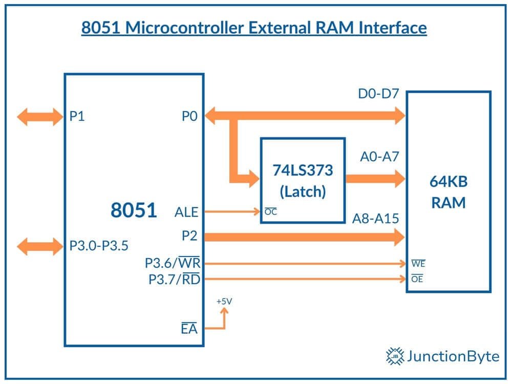
Note that the EA pin is connected to VCC, indicating that the Program Memory is internal. In the previous case (Interfacing External Data Memory (RAM) with 8051 Microcontroller), the EA Pin is connected to GND.
Since the Program Memory here is Internal (on-chip), the PSEN pin isn’t useful (can be left open).
External Program and Data Memories
It is possible to connect both External Program Memory and External Data simultaneously with the 8051 Microcontroller. Depending on how you use the Internal Program Memory, the EA Pin must be connected to VCC or GND.
If EA is connected to VCC, the CPU of the 8051 Microcontroller accesses the initial 4K addresses from Internal Program Memory and the remaining 60K addresses from External Program Memory.
The following image shows a Block Diagram of Interfacing External Program and Data Memories with 8051 Microcontroller.

The CPU differentiates between Internal and External RAM by the instructions we use (MOV for Internal RAM and MOVX for External RAM). I will explain the 8051 Microcontroller Instruction Set and Addressing Modes in separate guides.
Conclusion
This was a very lengthy and detailed guide on the 8051 Microcontroller Memory Organization. Here, I discussed the on-chip Program and Data Memories (ROM and RAM), how to interface external Program and Data Memories, how the CPU uses Ports as External Bus, and various External Bus Control Signals.
Continuing this Introductory Series on 8051 Microcontroller, I will explain a very important topic, the 8051 Microcontroller Special Function Register (SFRs) in the upcoming guide.